
1. What is Digital Chip Design?
At its core, digital chip design is the discipline of translating high-level human logic or mathematical algorithms into physical semiconductor structures capable of manipulating electrical signals at gigahertz frequencies. Modern microprocessors do not consist of hand-drawn transistors. Instead, hardware engineering operates through a strict hierarchy of abstraction layers:
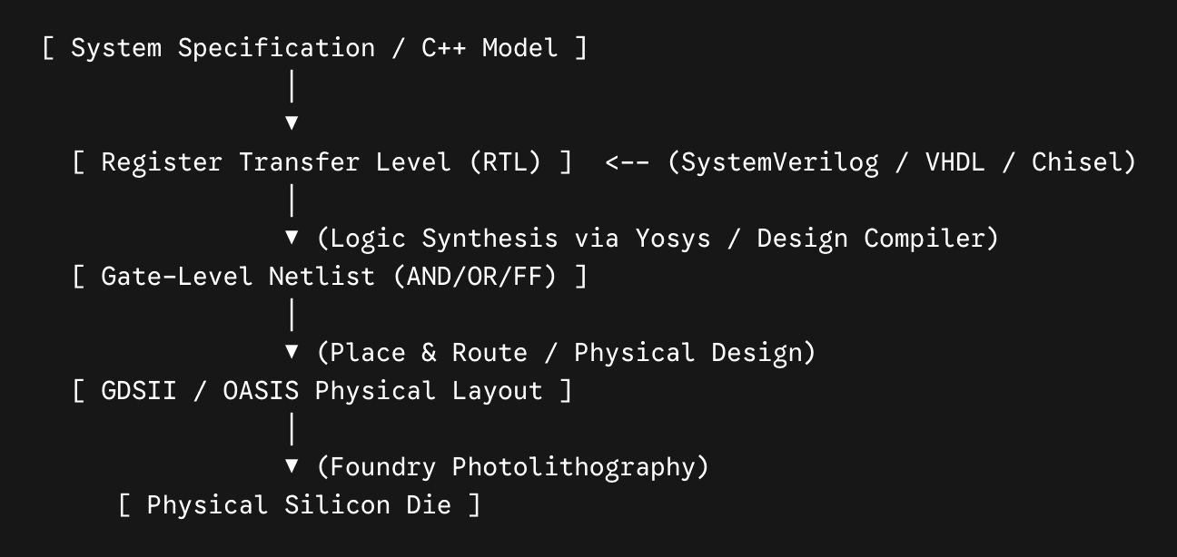
System Specification: Defining functional requirements, memory bandwidths, and power envelopes (often modeled in Python or C++ Golden Models).
Register Transfer Level (RTL): Describing data movement between hardware registers across clock cycles using Hardware Description Languages (HDLs) like SystemVerilog, VHDL, or Chisel.
Logic Synthesis: Translating high-level RTL code into a boolean netlist of standard logic gates (NAND, NOR, Flip-Flops) for a specific silicon process node (e.g., TSMC 3nm, Intel 18A, SkyWater 130nm).
Physical Design (Place & Route): Arranging standard cell gates on physical silicon floorplans and routing microscopic copper interconnections.
Mask Generation & Fabrication: Exporting physical layout files (GDSII or OASIS) to print photolithographic masks used to etch silicon wafers.
2. The 2026 Silicon Spectrum: ASICs, FPGAs, SoCs, and Chiplets
Not all silicon is fabricated the same way. Choosing the target architecture defines your upfront Non-Recurring Engineering (NRE) costs, manufacturing lead times, and verification complexity.
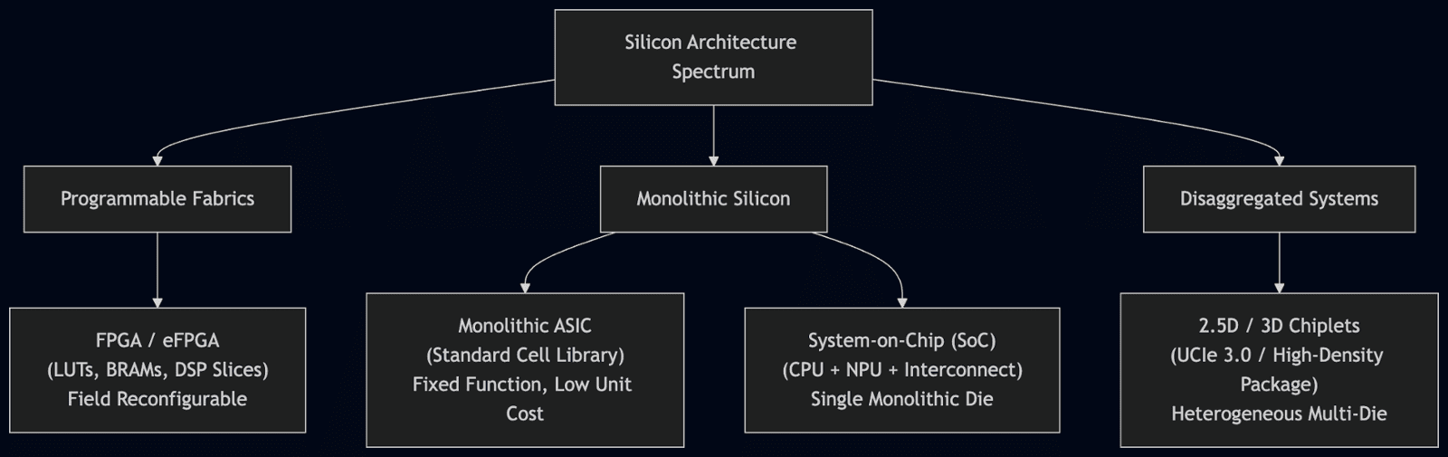
A. Field-Programmable Gate Arrays (FPGAs)
Architecture: Reconfigurable matrices of Look-Up Tables (LUTs), Configurable Logic Blocks (CLBs), Block RAM (BRAM), and DSP slices.
Trade-Off: $0 NRE cost and instant hardware reconfigurability, but higher power consumption and lower maximum frequency ($f_{MAX}$) compared to custom ASICs.
B. Monolithic Application-Specific Integrated Circuits (ASICs)
Architecture: Fixed-function transistors etched permanently onto a single silicon die using custom mask sets.
Trade-Off: Unmatched performance-per-watt and low per-unit manufacturing costs at scale, offset by massive upfront NRE costs ($10M–$100M+) and 6–12 month fabrication cycles.
C. Systems-on-Chip (SoCs)
Architecture: Integrating compute blocks (CPUs, GPUs, AI NPUs), memory controllers, and system buses (AMBA AXI/AHB) into a single monolithic die.
Trade-Off: Ideal for mobile and automotive platforms, but verification complexity grows exponentially as clock domains, reset paths, and power states interact.
D. Disaggregated Chiplets (2.5D/3D Integration):
Architecture:Replacing massive monolithic dies with smaller, specialized dies ("chiplets") mounted on a silicon interposer or organic substrate using standardized die-to-die interfaces like UCIe (Universal Chiplet Interconnect Express).
Trade-Off: Bypasses monolithic yield limits and allows mixed-process integration (e.g., a 3nm Compute Chiplet paired with a 12nm I/O Die), but introduces catastrophic system-level verification challenges across die boundaries.
3. The Crisis: Why Conventional Verification is Failing
For three decades, the semiconductor industry relied on a standard verification playbook: SystemVerilog + UVM (Universal Verification Methodology) + Constrained-Random Simulation + Human Waveform Debugging. In 2026, this legacy paradigm has officially hit a wall.
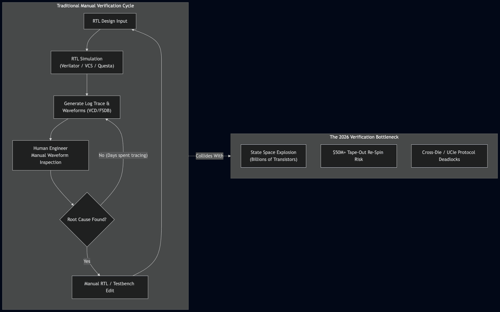
The 4 Pillars of the Verification Bottleneck
Slow Cycle-Accurate Simulation: RTL simulators are inherently sequential software programs trying to simulate parallel physical hardware. Running long regression suites for complex SoCs takes days or weeks, stalling engineering progress.
The Human Debug Bottleneck: Finding that a bug exists takes seconds during simulation; finding why it occurred requires a human engineer to manually trace signals across thousands of clock cycles in waveform dumps (.vcd / .fsdb).
Compositional Failure in Chiplets: An IP block or chiplet die may pass 100% of its isolated unit tests. However, when connected via UCIe links, asynchronous timing shifts, protocol latency mismatches, and shared power delivery networks trigger dormant deadlocks that standard block-level testbenches never predict.
4. The Cost of Failure: Silicon Doesn't Have Hotfixes
In cloud software engineering, a broken deployment is reverted in minutes with a git revert. In silicon engineering, a post-tapeout functional bug means:
$10M to $50M+ in destroyed photomask sets.
6 to 9 months of delayed market entry (often killing a startup or missing a product window entirely).
Catastrophic field failures if hardware bugs slip into automotive, medical, or aerospace systems.
Verification is no longer just a phase in the CAD workflow—it is the strategic bottleneck of modern semiconductor survival.
5. The Road Ahead: Autonomous & Closed-Loop Verification
To break through the verification wall, hardware engineering must move past fragile, human-intensive debugging loops.
The future belongs to Closed-Loop Telemetry Automation—where simulation engines, static formal analyzers, and domain-aware AI agents interact dynamically:
Automated Log & Waveform Parsing: AI telemetry engines ingest simulation logs, isolate exact signal transitions, and identify failure root causes in minutes.
Intelligent Test Generation: Moving away from dumb constrained-random sweeps toward coverage-driven, target-seeking test generation.
Self-Healing Verification Pipelines: Automatically feeding error telemetry back to design engines to iterate fixes before a human engineer ever opens a waveform viewer.